Large-area wafer-scale few-layer 2D MoTe 2 and MoS 2 grown on sapphire and silicon substrates by chemical vapor deposition
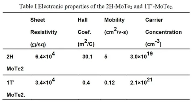
Figure I (a) Typical photograph of a 2-inch wafer with several layers of 2H-MoTe 2 films grown on a 2-inch SiOy/Si composite substrate (left-hand side). The middle wafer shows several layers of 2H-MoTe 2 films grown on a sapphire substrate. The wafer on the right shows IT’-MoTe 2 , a multilayer film grown on a sapphire substrate. (b) Raman spectrum of 2H-MoTe 2 grown on a 2-inch sapphire substrate.Figure 2 (a) 4-inch sapphire substrate (left), multi-layer IT’-MoTe 2 film grown on the 4-inch sapphire substrate (middle) and multi-layer IT’-MoTe 2 Typical photos of the film (b) Raman spectrum of the 1T’-MoTe 2 film grown on a 4-inch sapphire substrate.Based on the resulting peaks, our study concluded that MoTe 2 is in the 2H phase. Previous research by Fraser et al. The number of layers of 2H-MoTe 2 was indirectly determined by analyzing the Raman peak positions of E 2 g and B 2 g. In our study, atomic force microscopy examination of 2-inch wafers confirmed that the 2H-MoTe 2 film consists of five layers. We also observed the photo of a few-layer 1T’-MoTe 2 film grown on a 4-inch sapphire and SiO 2 sapphire composite substrate as shown in Figure 2(a) . The peaks at 267 and 162 cm -1 correspond to the Ag and Bg mode peaks, respectively, indicating that this MoTe 2 is the 1T’ phase. Furthermore, Raman spectra obtained from five spots on the wafer demonstrate acceptable material quality and thickness uniformity for few-layer 1T’-MoTe 2 films grown on sapphire. Based on Raman spectroscopy analysis, these wafers exhibit satisfactory within-wafer uniformity. In addition, our team has also developed the patterning of few-layer MoTe 2 and MoS 2 films through traditional photolithography and chemical etching techniques. The photolithography and etching processes form MoTe 2 steps, as shown in Figure 3.Figure 3 Typical photos taken from patterned few-layer 2H- and 1T’-MoTe 2 films using standard photolithography and chemical etching techniques.Hall effect measurements are used to determine the electrical properties of 2H-MoTe 2 and 1T’-MoTe 2 . The results are listed in Table I. The films exhibit p-type behavior and their electronic properties remain stable even after weeks of storage in the atmosphere. 1T’-MoTe 2 thin film has semi-metallic properties, relatively low Hall mobility and high hole concentration. Our study also analyzed the Raman spectrum of MoS 2 excited by 532nm laser. As shown in Figure 4, two modes were identified: the in-plane E 2 g mode and the out-of-plane A 1 g mode. These modes are located at 386 and 406 cm -1 respectively. The presence of these peaks confirms that MoS 2 is in a multilayered state. According to Li et al., the separation between these two modes decreases with decreasing material thickness, which indicates the number of layers of MoS 2 [10]. An atomic force microscope was used to analyze the prepared 2-inch wafer, and it was found that the MoS 2 few-layer film has 1-5 layers, which can be precisely controlled by adjusting the growth conditions. In our laboratory, we have developed the use of cold wall CVD methods to produce wafer-scale and few-layer continuous thin films of 2H-MoTe 2 and 1T’-MoTe 2 on silicon and sapphire substrates growth process. Raman spectroscopy and AFM surface morphology analysis confirmed that the crystalline phase and thickness of these films were uniform. The thickness of the film can be controlled between 3-6 nm. Hall effect measurements show that few-layer films of 2H-MoTe 2 and 1T’-MoTe 2 exhibit semiconducting and semimetallic properties, respectively. We are currently analyzing their properties and potential applications, and we welcome collaboration with researchers or teams interested in studying advanced devices or fundamental physics topics related to 2D TMDs.Figure 4 Typical Raman spectra of few-layer and single-layer MoS 2 grown on 2-inch sapphire and SiO 2 /Si substrates. The inset shows a typical photo taken by our team of few-layer MoS 2 grown on a sapphire substrate.
Development of Infrared Semiconductor Detectors Based on Tamm Plasmon Resonance
Photocatalytic Hydrogen Production and Carbon Dioxide Conversion to Formic Acid Using Nano Transition Metal Oxide Coupled Compound Semiconductors
Development of AlGaN Field-Effect Transistors (FETs)
Semiconductor High-Sensitivity Gas Sensor
Address: Rm. 48414, 4F., B201 Building, Cheng-Kung Campus, No. 1, University Rd., East Dist., Tainan TEL: 06-2757575 #63917Address: Rm. 49106B, 1F., B202 Building, Cheng-Kung Campus, No. 1, University Rd., East Dist., Tainan TEL: 06-2757575 #63906 #1062