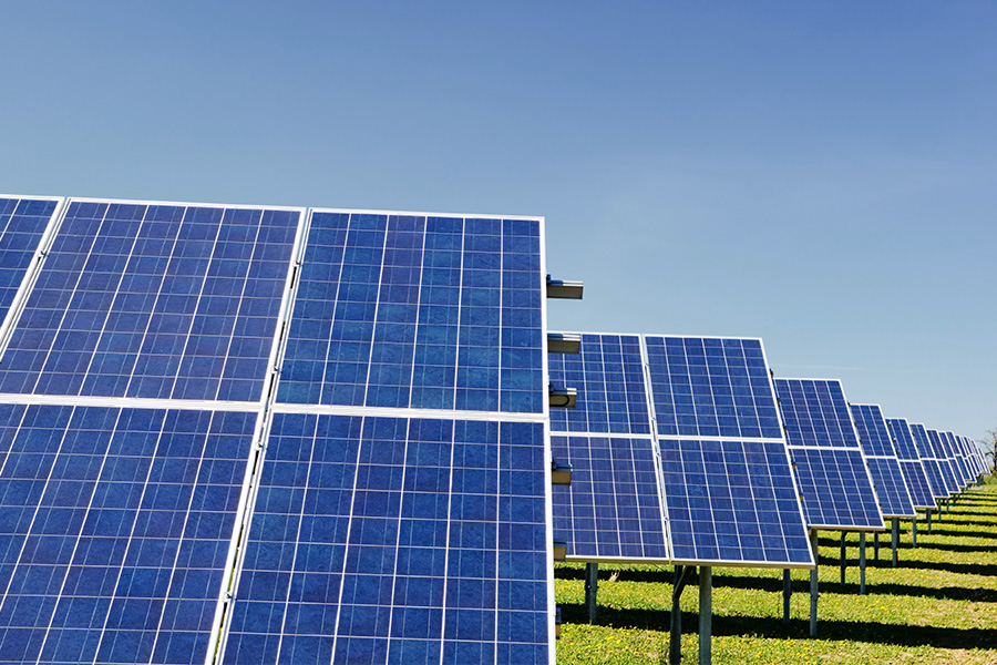
In recent years, Dr.Sheu’s team has achieved representative results in the research of intermediate band solar cells, photoelectrochemical hydrogen production, conversion of carbon dioxide to formic acid, AlGaN-based FETs, high-efficiency light-emitting diodes, and photodetectors. A brief summary of their ongoing projects is as follows.
In terms of future green energy technology, the applicant has devoted itself to the research of intermediate band solar cells in recent years, through...
In terms of future green energy technology, applicants have many types of materials that can be used as working electrodes for photoelectrolysis of water to produce hydrogen, such as: oxides...
In order to improve power conversion efficiency, FET components are traditionally used as switching components in power conversion (such as AC-DC converters), so...
Research on the development of replacement patterned sapphire substrate (PSS): PSS substrate is now the most popular one in various countries in China...
In response to the development of 5G and big data, the importance of near-infrared light detectors (NIR PD) has increased with the emergence of ...
Address:
Rm. 48414, 4F., B201 Building, Cheng-Kung Campus, No. 1, University Rd., East Dist., Tainan
TEL: 06-2757575 #63917
Address:
Rm. 49106B, 1F., B202 Building, Cheng-Kung Campus, No. 1, University Rd., East Dist., Tainan
TEL: 06-2757575 #63906 #1062
In terms of future green energy technology, the applicant has devoted itself to the research of intermediate band solar cells in recent years. Through manganese doping technology, a gap energy formed by impurity energy levels is created between the energy gaps of gallium nitride materials. This gives the solar cell the opportunity to absorb photons with energy smaller than the energy gap of the host material, thus improving the efficiency of the cell. In this regard, we are the first laboratory known in the world to experimentally confirm that manganese-doped gallium nitride can form a significant gap band photoelectric response, and this result has been applied to improve the efficiency of gallium nitride solar cells. According to research, currently only the laboratory led by me in China has the ability to grow this high-quality manganese-doped gallium nitride film with device grade. The figure below shows the intermediate band photoelectric response of the manganese-doped gallium nitride film. Penetration diagram. Relevant research has been published in Appl. Phys. Lett., 103, 063906 (2013) Scientific Reports, 8, 8641 (2018), etc.
In this study, under 1-sun AM1.5G illumination, AlGaN/GaN heterostructure solar cells with Mn (manganese) doping demonstrated 5 times the photocurrent compared to components without Mn doping. , the significant increase in conversion efficiency can be attributed to the light absorption caused by the energy state associated with manganese, thereby contributing additional photocurrent. From the analysis of the electroluminescence spectrum and spectral response characteristics obtained from manganese-doped components, as shown in the figure below, in the AlGaN/GaN absorption layer, the Mn-related energy state forms an intermediate band (Intermediate Band) within the energy gap. This gap energy The band causes subband gap absorption, thereby increasing the short-circuit current of AlGaN/GaN heterostructure solar cells. Please see Solar Energy Materials and Solar Cells, Vol. 157, 727–732 (2016) for details.
在未來綠色能源科技方面,本實驗室近年來致力於間隙能帶(intermediate band)太陽能電池之研究,透過錳摻雜技術在氮化鎵材料能隙間營造一個由雜質能階所形成之間隙能帶,這讓太陽能電池有機會吸收能量小於主材料能隙的光子,進而提升電池之效率。目前在這方面,我們是已知在全世界首次以實驗證實錳摻雜氮化鎵具有形成顯著間隙能帶光電響應之實驗室,並將此一結果應用於提升氮化鎵太陽能電池之效率的研究,目前本實驗室有能力成長此一具有元件等級之高品質錳摻雜氮化鎵薄膜,下圖所示為錳摻雜氮化鎵薄膜所展現之中間能帶光電響應穿透圖。相關之研究已發表在Appl. Phys. Lett., 103, 063906(2013) Scientific Reports, 8, 8641 (2018) 等。
在這方面的研究中,在1-sun AM1.5G光照條件下,與沒有Mn摻雜的元件相比,具有Mn(錳)摻雜的AlGaN / GaN異質結構太陽能電池展現了5倍光電流,其轉換效率的顯著提升可歸因於與錳相關的能量狀態所引起的光吸收有關,並據此貢獻額外的光電流。從摻錳元件獲得的電致發光光譜和光譜響應特性分析得知,如下圖所示在AlGaN / GaN吸收層內,Mn相關能態在能隙內形成間隙能帶(Intermediate Band),此間隙能帶引起subband gap absorption,進而增加AlGaN / GaN異質結構太陽能電池之短路電流。請詳見Solar Energy Materials and Solar Cells, Vol. 157, 727–732 (2016)。
There are many types of materials that can be used as working electrodes for photoelectrolysis of water to produce hydrogen, such as oxides or low-energy-gap semiconductors. However, in practical applications, these oxides are limited by the limited available solar spectrum, resulting in low photoelectric conversion efficiency during photoelectrolysis of water, and low energy gap semiconductor materials, such as indium phosphide, gallium arsenide, and cadmium selenide. , although they can absorb sunlight more effectively, these materials are easily corroded by acidic or alkaline solutions. The gallium nitride series of materials is a feasible and promising material for photoelectrolysis of water because its band edge potential can not only meet the needs of photoelectrolysis of water, but also has good corrosion resistance. In addition, the energy gap size can be changed by changing the composition ratio of indium gallium nitride (InxGa1-xN). This topic is the study of photoelectrolysis of water using an indium nitride working electrode to simultaneously produce hydrogen (H2) and convert carbon dioxide into formic acid (HCOOH). Formic acid is an important industrial raw material and a potential hydrogen storage molecule. It contains It contains more hydrogen than other storage solutions, and the decomposed hydrogen can be used directly without purification. In the research field of converting carbon dioxide using artificial photosynthesis, it is still faced with low efficiency and low stability. , and photocorrosion and other problems need to be solved. Indium gallium nitride series materials have a direct energy gap, high resistance to acid and alkali corrosion, and a conductive band higher than the potential of carbon dioxide reduction to formic acid. They can not only be used for photoelectrolysis of water to produce hydrogen but also convert carbon dioxide to produce formic acid. However, because their energy gap is too large , can only absorb a small part of the solar spectrum, and the conversion efficiency is limited. If you want to increase the conversion efficiency under the same lighting environment, you must increase the number of cathode photoelectrons, that is, increase the photocurrent of the overall reaction. One method is to increase the amount of photogenerated carriers in the semiconductor photoanode. We use double-sided epitaxial technology to grow InGaN/GaN on a double-sided polished sapphire substrate. Si-doped InGaN and GaN layers are grown on both surfaces of the sapphire substrate respectively. The photoelectrode produced by this method can increase light Absorption amount. In addition to this, the electrolyte used in this study was a mixture of NaCl and water, which is an environmentally friendly aqueous solution rather than a man-made acid or alkali solution such as HCl or KOH. This study uses salt water as the electrolyte, which opens a window for using sea water as the electrolyte in the future. After this technology enters the practical stage in the future, filtered sea water can be directly used as the electrolyte required for the reaction, which will be more environmentally friendly and Economy. This paper is the first time in the literature to reveal this design. InGaN and GaN layer double-sided epitaxial wafers are made into working electrodes, showing higher hydrogen production and CO2 reduction rate. The conversion efficiencies of HCOOH and H2 are estimated to be 1.09% and 5.48% respectively. The former is much higher than the photosynthesis of plants, which provides a potential solution for reducing carbon dioxide levels in the atmosphere. Please see Solar Energy Materials and Solar Cells, Vol. 157, 727–732 (2016) and Solar Energy Materials and Solar Cells, Vol.202, 110153–90 (2019) for details.
In order to improve power conversion efficiency, FET components have traditionally been used as switching components for power conversion (such as AC-DC converters), and Enhanced-mode FETs are the main ones. In recent years, the demand for Enhanced-mode GaN FET has increased rapidly, but there are still some bottlenecks in its production. The most common Enhanced-mode GaN FET must have a p-GaN gate layer. For the regrowth or patterning etching of p-GaN in the gate region, hydrofluoric acid (HF) acid etchant is often used to make a thin dielectric film SiO2 or The mask layer composed of SiNx is patterned, and the remaining mask layer is removed after epitaxial regrowth. However, during the regrowth process, impurity contamination caused by the out-diffusion of mask materials (such as SiO2 or SiNx) will lead to a decrease in crystal quality. This study demonstrates an AlGaN/GaN heterostructure field effect transistor (HFET), whose technical feature is to use Si ion implantation in the drain and source regions as a mask layer, through selective area epitaxy regrowth technology Forming a p-GaN gate layer overcomes the shortcomings of conventional designs and improves crystal quality, thereby making the FET more power-saving and further improving power conversion efficiency.
Research on the development of replacing patterned sapphire substrate (PSS): PSS substrate is now a necessary raw material for major domestic gallium nitride LED die manufacturing companies in the epitaxial growth wafer process, because compared with traditional flat surfaces The sapphire substrate is expected to increase the power of LED chips by at least 40%, but the relevant patents are held by major foreign manufacturers, such as Nichia, Mitsubishi and Lumileds. The main claim of these patents is to emphasize that the surface of the sapphire substrate has an undulating pattern, so that after the growth of the gallium nitride LED epitaxial layer, a roughened GaN/saaphire interface (as shown in the schematic diagram in Figure 1) is obtained to facilitate photons. The scattering thereby increases the light extraction efficiency. The applicant uses ion implantation to produce a substantially planarized substrate, which is different from the traditional PSS substrate that has an uneven surface. The gallium nitride epitaxial film is directly formed on a sapphire substrate where the crystal lattice has been destroyed in a local area, so that selective growth occurs between the semiconductor epitaxial layer and the substrate, and holes are generated at this interface to promote light scattering ( (As shown in the schematic diagrams in Figures 2 and 3), thereby improving the luminous efficiency of blue LEDs. This technology can replace the traditional PSS substrate and break through the patent barriers of foreign manufacturers. Relevant research has been published in academic journal papers [1-6]. On the other hand, in recent years, the applicant has used the photon-recycling structure as the core, by superposing a semiconductor quantum well conversion layer on the electrical pumping luminescent quantum well, hoping to use the quantum well conversion layer to Replace phosphors to make white LEDs. When current is injected into this structure, the high-energy (short-wavelength) photons emitted by the electroluminescent quantum wells are absorbed by the conversion layer and released into photons of different wavelengths, thereby forming a white light spectrum to replace the traditional multi-color LED die combination. white LED or phosphor white LED. In terms of device design, the energy gap of the electrically excited light quantum well layer in the lower part of the epitaxial structure is usually larger than the energy gap of the upper light excited light quantum well conversion layer, so that electrically excited photons with higher energy can be The narrow energy gap light excitation light conversion layer is absorbed, so that the device can achieve the purpose of photon recycling effect. With this design concept, the applicant has produced a single crystal grain with four wave peaks composed of low color temperature and high temperature. High-efficiency white light-emitting diodes with color rendering coefficient. Figure 4 shows the luminescence spectrum of a representative white LED with low color temperature and high color rendering coefficient. Relevant research has been published in related journals such as Optics Express and IEEE TED.
Traditional phosphor white LEDs include blue LEDs and yellow phosphors. The blue LED emits blue light to excite the yellow phosphor, while the yellow phosphor absorbs part of the blue light and is excited to produce yellow light, which then mixes with other parts of the blue light. Combined into a double-peak white light spectrum, it is difficult to achieve high color temperature and high color rendering coefficient. In recent years, white LEDs have been considered to have great potential as light sources for visible light communication (VLC) systems. Because LEDs are based on the emission of semiconductors, they can be modulated significantly faster than traditional incandescent or fluorescent light sources and can be integrated with the electronics that drive them. Current LED-based VLC systems usually use traditional phosphor white LEDs, which usually only have an electro-optical (E-O) modulation bandwidth of the order of 10-20MHz. Therefore, traditional white LED applications still encounter many challenges in the VLC field. . Currently, the methods of producing white LEDs are divided into two categories. One is a phosphor white LED, and the other is a white LED made of a combination of red, green, and blue LED chips. Traditional phosphor white LEDs include blue LEDs and yellow phosphors. The blue LED emits blue light to excite the yellow phosphor, while the yellow phosphor absorbs part of the blue light and is excited to produce yellow light, which then mixes with other parts of the blue light. combine to form white light. Generally speaking, the luminescence mechanism of phosphors excited by light is phosphorescence, and the life cycle of phosphorescence is about 10-3 to 102 seconds. Therefore, the modulation frequency of the light frequency emitted by phosphors The Modulation Bandwidth is limited, generally no more than 10MHz. Therefore, it is difficult for phosphor white LEDs to be directly used in high-bit-rate data transmitters in visible light communication systems. It is usually necessary to add a filter to remove the light emitted from yellow phosphors. Yellow-green light filtering. On the other hand, compared to phosphor white LEDs, the white light emitted by white LEDs composed of red, green, and blue LED chips has an overall modulation bandwidth that is not affected by the slow response of fluorescent white LEDs. Affected by the powder, it can provide a higher modulation bandwidth, so it can be used in high bit rate data transmitters and lighting devices. However, from a cost perspective, white LEDs are composed of three different LEDs: red, green, and blue. The number and types of LEDs required are large, so the driving circuit of this kind of white LED is also complicated. It is more complex and therefore more expensive. Furthermore, due to the different life cycles of the three types of LEDs, after a period of use of this kind of white LED, the reliability of the color temperature performance of the white LED will decrease, and it is necessary to use a color sensor to correct the white light and change the initial driving conditions to achieve the desired performance. The white color temperature of the initial white LED. Therefore, developing a lower-cost white light LED that is suitable for VLC communication systems is one of the problems that current researchers are eager to solve. The photon recycling structure LED developed by the applicant in recent years has the potential to become a white LED light source used in VLC systems, because such a design can eliminate the need for slow-response phosphors and directly stack green, blue or red colors through epitaxial growth. Quantum wells play the role of phosphors in near-subtron external light luminescence, and achieve multi-wavelength luminous LEDs with a single crystal. Traditional series-connected single-crystal multi-wavelength LEDs are limited by the short hole diffusion length, making it difficult to achieve electrical pumping luminescence in all stacked quantum wells. The photon recycling structure developed by the applicant in recent years LED uses optical pumping to make all stacked quantum wells emit light. Therefore, the emission spectrum can be controlled by adjusting the thickness of each quantum well layer, and does not require multiple electrodes, multiple crystal grains or phosphor layers. The design will help improve the modulation bandwidth of white LEDs and be suitable for VLC communication systems. Appl. Phys. Lett. Vol.101, 151103(2012) 2. IEEE Electron Device Letters, Vol. 34, No.12, 1542(2013) 3. IEEE J. Quantum Electronics, Vol.48, No.8, 1004 (2012) 4. Appl. Phys. Lett. Vol.101, 151103(2012) 5. IEEE Electron Device Letters, Vol. 34 No. 12, 1542(2013) 6. ACTA Materialia, Vol.107, 17(2016) .
In response to the development of 5G and big data, the importance of near-infrared light detectors (NIR PDs) has increased with the emergence of self-driving cars and robots. However, there is currently a lack of NIR PDs with high responsiveness and narrow bandwidth on the market. We Through the combination of Tamm Plasmons Resonance (TPR) and metal-semiconductor-metal (MSM) structure, the foundation is established for producing NIR PD with both high responsivity and high wavelength selectivity.
This research uses a Bragg reflector (DBR) composed of oxide dielectric (such as silicon dioxide/titanium dioxide) or AlxGa1-xAs/AlyGa1-yAs, plus a thin metal film to promote TPR, and combines it with an MSM structure to produce an electrode. Narrow bandwidth NIR PD. First, we study the production of Bragg reflectors and metal films on sapphire or gallium arsenide substrates, and analyze the optical characteristics of TPR combined with metal-semiconductor-metal structures, confirm and establish the relevant TPR modeling parameters, and then produce PD elements for optoelectronics. Measure. Then, two-dimensional materials are used as the active layer of the metal-semiconductor-metal structure, and TPR is used to analyze and study the gain. Since traditional semiconductor thin film materials are deposited on lattice-mismatched material layers (such as gold), they will produce more Structural defects lead to high component dark current and thus affect component performance. In order to overcome this problem, we mainly use two-dimensional semiconductor materials to replace traditional bulk materials as active layers. Since most of them are single-layer or few-layer Two-dimensional materials are vertically stacked with other material layers only through van der Waals forces. Therefore, in theory, there will not be too many structural defects due to lattice mismatch. It is expected that device performance can be improved accordingly. Since the material layers are vertically stacked with other materials only through van der Waals forces, the impact of the carrier transport capability and mechanism between layers on the performance of the core components of this study is the focus of research, especially the plasma Caused by the transfer process of hot carriers between layers. Therefore, we use the reliable components produced by our accumulated experience as carriers to focus on exploring the phenomenon of carrier transmission.