Current research
Large-area wafer-scale few-layer 2D MoTe2 and MoS2 grown on sapphire and silicon substrates by chemical vapor deposition
In recent years, 2D materials have been extensively studied. The most common method of preparing these materials into several layers or into a single layer is mechanical exfoliation. However, it is difficult to transfer large-area films using this method, which is challenging for practical process applications. To overcome these limitations and produce large-area continuous thin films of two-dimensional materials, chemical vapor deposition (CVD) has been extensively studied. Several publications demonstrate the successful use of CVD for the production of MoS2, MoSe2, WS2, and WSe2.
MoTe2, also known as molybdenum ditelluride, is a member of the transition metal dichalcogenide (TMD) family and has attracted attention due to its interesting physical properties [1]. It is a semiconductor material with a similar energy gap to silicon (Si), making it a promising candidate for next-generation integrated circuits (ICs) [3]. In addition, MoTe2 possesses a range of other fascinating properties such as topological insulator, Weyl semimetal and superconductor [1].
In recent years, two-dimensional (2D) heterogeneous homogeneous junctions have become increasingly popular, which consist of a crystal structure of a semiconductor phase and a crystal structure of a semimetallic phase. Few-layer MoTe2 is considered a potential material for this application [2]. The homojunction composed of metallic phase and semiconductor phase MoTe2 can also be used to solve the problem of large contact resistance in field effect transistors [7]. In addition, the electrical properties of MoTe2 can be adjusted through the oxidation of its surface layer, making MoTe2 attract attention [6].
MoTe2 has at least two distinct phases: a diamagnetic semiconductor phase (α) and a metal-containing paramagnetic phase (β). The homogeneous region where the two phases coexist is between MoTe1.90 and MoTe1.99 . The transition temperature is 820°C for the Te-rich sample and 880°C for the Mo-rich sample [9]. .
However, despite its potential, there have been few studies on growing large-area, high-quality, few-layer MoTe2 via CVD. This is because it is very challenging to produce continuous thin films of a single pure phase. MoTe2 is a phase change material that can develop into two different phases according to epitaxial growth conditions, 1T’-MoTe2 (β) and 2H-MoTe2 (α). Both phases have unique properties and are used in different fields.
Our laboratory has been using cold wall chemical vapor deposition (CWCVD) to grow large-area 1T’-MoTe2 and 2H-MoTe2 films on various substrates. So far, we have successfully grown few-layer continuous films of 1T’-MoTe2 and 2H-MoTe2 on 2-inch or 4-inch silicon and sapphire substrates. Remarkable results have been achieved. These films typically have a thickness of 3 to 5 layers. In addition, we vertically stacked heterogeneous homogeneous junctions made of 1T’-MoTe2 and 2H-MoTe2 by adjusting the growth parameters.
The CWCVD system used in our study consists of a main reactor with an overhead nozzle and a 4-inch diameter rotating base with a heating coil. Two independent small furnace tubes are connected to the main reactor, in which MoO3, WO3, Ga2O3 are inserted Precursor powders such as Te and Te are placed outside the reactor. Carrier gases such as Ar and H2 are used to deliver the precursors to the main reactor. To produce sulfide-based materials, H2S gas is used as the hydride source.
In order to prepare MoTe2 films with various crystal phases, the reactor pressure was adjusted to 50-200 Torr and the stage temperature was set between 450-550°C. The temperature of the furnace tube is set to 650℃ and 550℃ respectively to vaporize MoO3 and Te powder. A mixture of Ar and H2 is mixed with MoO3 and Te vapors and then reaches the substrate surface via a spray nozzle. The concentrations of MoO3 and Te vapors were controlled using a mass flow controller (MFC). Adjust the evaporation temperature of MoO3 and Te powder, the gas flow rate of Ar and H2 , and the reactor pressure to adjust the phase of the MoTe2 film. The thickness uniformity of the MoTe2 film can be optimized by changing the rotation speed of the base and the distance between the substrate and the nozzle. The image in Figure 1(a) shows typical photos of 2H- and 1T’ few-layer films – MoTe2 grown on 2-inch SiO2/Si composite and sapphire substrates. The Raman spectrum of 2H-MoTe2 excited by a 532 nm laser is shown in Figure 1(b). The peaks observed at 235, 171 and 287 cm-1 correspond to in-plane E2g, out-of-plane A1g and Out-of-plane B2g mode peak.

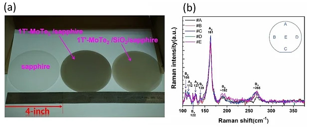
Figure 2 (a) 4-inch sapphire substrate (left), multi-layer IT’-MoTe2 film grown on the 4-inch sapphire substrate (middle) and multi-layer IT’-MoTe2 Typical photos of the film (b) Raman spectrum of the 1T’-MoTe2 film grown on a 4-inch sapphire substrate.


Development of Infrared Semiconductor Detectors Based on Tamm Plasmon Resonance
Photocatalytic Hydrogen Production and Carbon Dioxide Conversion to Formic Acid Using Nano Transition Metal Oxide Coupled Compound Semiconductors
Development of AlGaN Field-Effect Transistors (FETs)
Semiconductor High-Sensitivity Gas Sensor
Compound Semiconductor and Applied Photonics laboratory
Department of Photonics Science
National Cheng Kung University
Professor Jinn-Kong Sheu's office
Address:
Rm. 48414, 4F., B201 Building, Cheng-Kung Campus, No. 1, University Rd., East Dist., Tainan
TEL: 06-2757575 #63917
Laboratory
Address:
Rm. 49106B, 1F., B202 Building, Cheng-Kung Campus, No. 1, University Rd., East Dist., Tainan
TEL: 06-2757575 #63906 #1062